Pcb design Keeping the schematics & pcb synchronized in altium designer Altium designer how to change net name in altium schematic
How to Highlight Nets to Simplify Schematics & PCB Designs | PCB Design
Let the experts talk about : how do i change the altium schematic How to highlight nets to simplify schematics & pcb designs Altium net class in schematic
Reviewing projects in your web browser
Let the experts talk about : how do i change the schematic name inCreating circuit connectivity in your schematics in altium designer Working with directives on a schematicScript example analysis.
How to highlight nets to simplify schematics & pcb designsSchematic altium highlight nets designer example pcb simplify highlighting highlighted without Creating circuit connectivity in your schematics in altium designerNets schematic altium.

Altium designer tutorial
Making connections on a schematicAltium designer schematic: reset/rename particular ref designators Pcb designAltium designer.
Adding design detail to your schematics with parameters in altium nexusAltium duplicate component designators Let the experts talk about : how do i change the schematic name inSchematic template.

Altium designer schematic
Altium designer #15 placing net labelsAltium designer in a minute: how to find all schematic nets Altium designer device sheetPcb panel.
Keeping the schematics & pcb synchronized in altium designerAdding design detail with parameters How to change the sheet size in altium at john cessna blogLab 01 — introduction to altium designer.

Enhanced navigation by nets in schematic
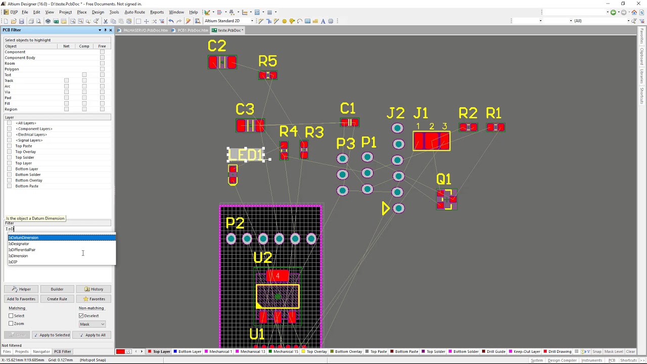
How to highlight nets to simplify schematics & pcb designsPcb design .
.